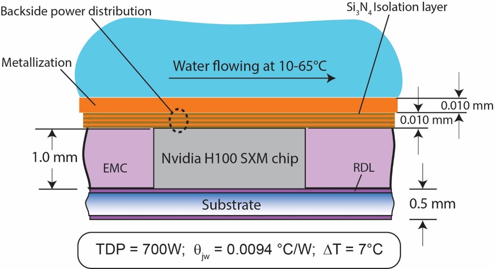
This thermal model is provided for one of the highest-powered components currently available, the Hopper H100 SXM chip from Nvidia that dissipates 700W. To a first approximation, heat flow need be considered in the vertical direction only; i.e., lateral heat spreading is ignored. Si3N4 layers are used to isolate conductive power distribution layers from the Hopper chip and from the metallization. The chip temperature is loosely clamped to the water temperature with a ΔT of around 7°C between them.
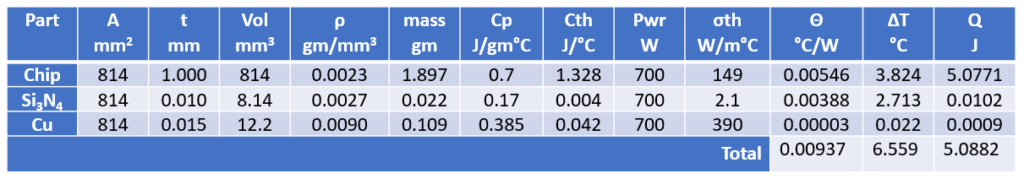
The Table is used to calculate ΔT, the temperature difference between transistor junctions and cooling water. A = area, t = thickness, Vol = volume, ρ = density, mass = inertial mass, Cp = specific heat, Cth = thermal mass, Pwr = power, σth = thermal conductivity, Ɵ = thermal resistance, ΔT = temp. diff., and Q = Cth.ΔT = transferred heat energy. Consider that in prior systems a package and a massive heat sink would be required to handle such a high-powered chip. Whatever the cooling path, 700W must be dissipated. The proposed design is disruptive because of low thermal resistance in the cooling path; this leads to high energy efficiency and low demand on cooling water.