This history is extracted from an SCV-EPS lecture given by John Lau of Unimicron Technology Corporation in Milpitas, California, on March 9, 2023.

2013
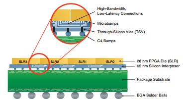
Xilinx was the first to implement a chiplet design, working with TSMC and employing their chip-on-wafer-on-substrate (CoWoS) 3D IC process. A large FPGA SOC was split into 4 smaller chips using 28 mm silicon; these were mounted on a silicon interposer using through-silicon vias (TSVs) and 4 levels of redistribution layers (RDLs). The RDLs had 0.4µm line width and spacing. Each FPGA had over 50,000 microbumps on a 45µ pitch. The package substrate was at least 5-2-5 and employed BGA solder balls.

2019
In 2019 AMD shipped their Extreme-perfomance yield computing (EPYC) device. A Core complex die (CCD) was split into 2 chiplets and fabricated by a 7nm process technology provided by TSMC; it is a stacked memory device. The I/O chip was fabricated by Global Foundries using 14 nm process technology. EPYC is a 2D IC integration.

2020
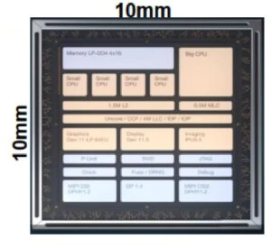
In 2020 Intel shipped their Lakefield device which included an active interposer, distinct from AMD’s EPYC which employed a passive interposer. It is a 3D IC integration. The memory and graphics are partitioned into multiple chips. A Large CPU has been partitioned into 5 smaller CPUs employing 10 nm process technology. The chiplets are attached to the interposer using face-to-face microbumps.

2021
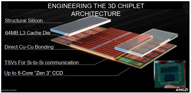
In 2021 AMD shipped their Ryzen 9 5900X prototype chip for gaming. It employed a V-Cache device employing bumpless hybrid bonding, i.e., direct copper-to-copper bonding. The process technology was 7nm from TSMC. This is a 3D IC integration.
The Moral of the Story
In each case cost was the driver. The economy derived from implementing silicon chips in smaller form factors far exceeded the additional packaging cost due to the requirement to connect all the smaller chips together.

